
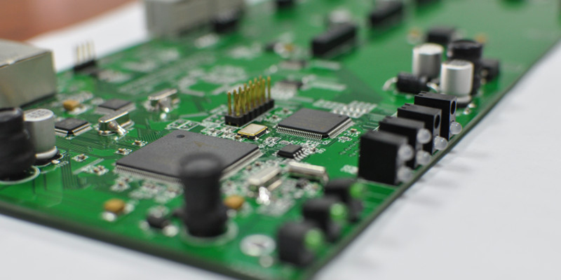
In the fast-evolving world of electronics manufacturing, Printed Circuit Boards (PCBs) serve as the backbone of virtually all modern electronic devices. As devices become increasingly compact and multifunctional, optimizing PCB design—specifically the board's dimensions and shape—has become critical for ensuring efficient and high-quality Surface Mount Technology (SMT) assembly. This article explores how different PCB sizes and shapes affect SMT processes, production stability, and cost-effectiveness.
How PCB Dimensions Influence SMT Assembly
1. Large PCB Sizes
Production Efficiency: Larger PCB panels typically require longer transfer times and higher positional accuracy during SMT assembly. For instance, a board with dimensions of 310mm x 410mm needs precise alignment when loaded into an SMT line to maintain placement accuracy. These extra alignment and handling steps can reduce the number of components placed per unit time, lowering throughput.
Stability and Accuracy: Large PCBs are more susceptible to thermal expansion, warping, and mechanical stress, particularly during reflow soldering. This can lead to component misalignment and increased defect rates. For example, a warped board may cause chips to be slightly off their designated pads, resulting in soldering defects. To mitigate this, proper PCB materials and board support designs, like using carriers or frame stiffeners, are essential. Learn more about handling large PCBs during SMT processing.
2. Small PCB Sizes
Efficiency and Placement Precision: Smaller PCBs generally support faster throughput as they require shorter transfer times and less repositioning. However, they present unique challenges due to their limited real estate and higher component density. For instance, 0201 components require extremely high placement accuracy, and even minor deviations can cause functional failures.
Panelization for Efficiency: To overcome size limitations, manufacturers often use panelization—combining multiple small boards into a single panel. This approach streamlines SMT placement and soldering, reducing the risk of board displacement during transport. However, careful attention must be given to V-groove or tab-routing designs to ensure smooth depaneling without damaging components.
Explore effective PCB panelization techniques for SMT.
With more than 5 years in the field of PCB prototype and fabrication, PCBYES is committed to supporting optimized board designs for both large and small-scale SMT production. Our skilled electronics engineers provide turnkey PCBA services with a focus on performance, cost, and delivery.
The Impact of PCB Shape on SMT Processing
1. Regular PCB Shapes
Rectangular or Square Boards: These are the most common shapes used in electronics manufacturing due to their compatibility with standard SMT equipment. Rectangular PCBs, such as a 150mm x 150mm board, provide predictable handling and alignment, making them ideal for high-density component placement. Their geometric simplicity ensures reliable transport, positioning, and repeatability throughout the assembly line.
Round or Polygonal Boards: Although less common, round or polygonal PCBs are prevalent in niche applications like wearable technology, where compact, ergonomic shapes are essential. However, such shapes often require custom fixtures and may introduce alignment challenges during SMT, especially if the boards rotate or shift during processing. These factors can reduce yield and increase setup time, unless robust clamping and positioning systems are used.
2. Irregular and Asymmetric PCB Shapes
Complex Form Factors: In some applications, such as aerospace, automotive, or medical devices, PCBs may be designed in asymmetric or custom shapes to fit within non-standard enclosures. These irregular PCBs require specialized tooling, such as custom SMT carriers or vacuum chucks, to maintain alignment during component placement and reflow soldering. Since these processes demand more sophisticated machinery and setup time, they often result in higher production costs.
Handling and Fixture Requirements: Boards with complex geometries are more prone to misalignment and mechanical movement during SMT operations. Misregistration can occur if the board shifts even slightly, requiring investment in higher-precision vision alignment systems. Manufacturers must also design board outlines with features that enable stable fixation, like fiducials or tooling holes.
Design Recommendations for Optimal SMT Assembly
To optimize SMT assembly regardless of board size or shape, PCB designers should consider the following:
Standardize PCB outline when possible to leverage existing SMT capabilities.
Incorporate panelization strategies for smaller boards to increase throughput and handling efficiency.
Use proper materials to ensure thermal and mechanical stability, especially for larger boards.
Include fiducials, tooling holes, and symmetric outlines to support accurate machine vision alignment.
Coordinate with assembly service providers early in the design phase to ensure compatibility with SMT production lines.
Read more about Boosting SMT production efficiency with better PCB design.
At PCBYES, we take pride in being not only your trusted PCB and PCBA supplier but also your partner in every stage of electronic manufacturing. Whether you're working with unique form factors or high-volume standardized designs, our solutions are tailored to match your technical and commercial goals.


